- 您现在的位置:买卖IC网 > Sheet目录1214 > EVAL-ADE7816EBZ (Analog Devices Inc)BOARD EVALUATION FOR ADE7816
�� �
�
�HSA� function� polarity� of� the� SS� /HSA� pin� during� communication.�
�ADE7816�
�HSDC� Interface�
�The� high� speed� data� capture� (HSDC)� interface� is� disabled� by�
�default.� It� can� be� used� only� if� the� ADE7816� is� configured� with�
�an� I� 2� C� interface.� The� ADE7816� SPI� interface� cannot� be� used�
�simultaneously� with� the� HSDC� port.�
�Bit� 6� (HSDCEN)� in� the� CONFIG� register� (Address� 0xE618)�
�activates� HSDC� when� set� to� 1.� If� the� HSDCEN� bit� is� cleared� to� 0,�
�the� default� value,� the� HSDC� interface� is� disabled.� Setting� the�
�HSDCEN� bit� to� 1� when� the� SPI� is� in� use� does� not� have� any� effect.�
�The� HSDC� port� is� an� interface� for� sending� up� to� four� 32-bit�
�words� to� an� external� device� (usually� a� microprocessor� or� a� DSP).�
�The� words� represent� the� instantaneous� values� of� the� currents� and�
�voltage.� The� registers� that� are� transmitted� are� IAWV/IDWV,�
�IBWV/IEWV,� ICWV/IFWV,� and� VWV.� All� are� 24-bit� registers�
�that� are� sign� extended� to� 32� bits.�
�The� HSDC� port� can� be� interfaced� with� the� SPI� or� similar� interfaces.�
�HSDC� is� always� a� master� of� the� communication� and� consists� of�
�three� pins:� HSA,� HSD,� and� HSCLK.� HSA� represents� the� select�
�signal.� It� stays� active� low� or� high� when� a� word� is� transmitted,�
�and� it� is� usually� connected� to� the� select� pin� of� the� slave.� HSD�
�sends� data� to� the� slave,� and� it� is� usually� connected� to� the� data�
�input� pin� of� the� slave.� HSCLK� is� the� serial� clock� line� that� is�
�generated� by� the� ADE7816� ,� and� it� is� usually� connected� to� the�
�serial� clock� input� of� the� slave.� Figure� 43� shows� the� connections�
�between� the� ADE7816� HSDC� and� slave� devices� containing� a� SPI�
�interface.�
�Data� Sheet�
�The� words� can� be� transmitted� as� 32-bit� or� 8-bit� packages.� When�
�Bit� 1� (HSIZE)� in� the� HSDC_CFG� register� is� 0� (the� default� value),�
�the� words� are� transmitted� as� 32-bit� packages.� When� Bit� HSIZE� is� 1,�
�the� registers� are� transmitted� as� 8-bit� packages.� The� HSDC� interface�
�transmits� the� words� MSB� first.�
�When� Bit� 2� (HGAP)� is� set� to� 1,� a� gap� of� seven� HSCLK� cycles� is�
�introduced� between� packages.� When� the� HGAP� bit� is� cleared� to� 0�
�(the� default� value),� no� gap� is� introduced� between� packages� and�
�the� communication� time� is� shortest.� In� this� case,� HSIZE� does�
�not� have� any� influence� on� the� communication,� and� a� data� bit� is�
�placed� on� the� HSD� line� with� every� HSCLK� high-to-low� transition.�
�For� correct� operation,� Bits[4:3]� (HXFER[1:0])� must� be� set� to� a�
�value� of� 01b.� The� words� representing� the� instantaneous� values�
�of� currents� and� voltage� are� transmitted� in� the� following� order:�
�IAWV/IDWV,� VWV,� IBWV/IEWV,� VWV,� ICVW/IFWV,� and�
�VWV,� followed� by� one� 32-bit� word� of� all� 0s.� Note� that� the� voltage�
�waveform� is� sent� three� times.� Bit� 14� (CHANNEL_SEL)� of� the�
�COMPMODE� register� (Address� 0xE60E)� can� be� used� to� select�
�which� group� of� current� channels� is� transmitted� (see� the�
��Bit� 5� (HSAPOL)� of� the� HSDC_CFG� register� determines� the�
�E�
�A� A�
�When� the� HSAPOL� bit� is� 0� (the� default� value),� HSA� is� active� low�
�during� the� communication.� This� means� that� HSA� stays� high�
�when� no� communication� is� in� progress.� When� the� communication�
�starts,� HSA� goes� low� and� stays� low� until� the� communication� ends.�
�Then� it� goes� back� to� high.� When� HSAPOL� is� 1,� the� HSA� function�
�of� the� SS� /HSA� pin� is� active� high� during� the� communication.�
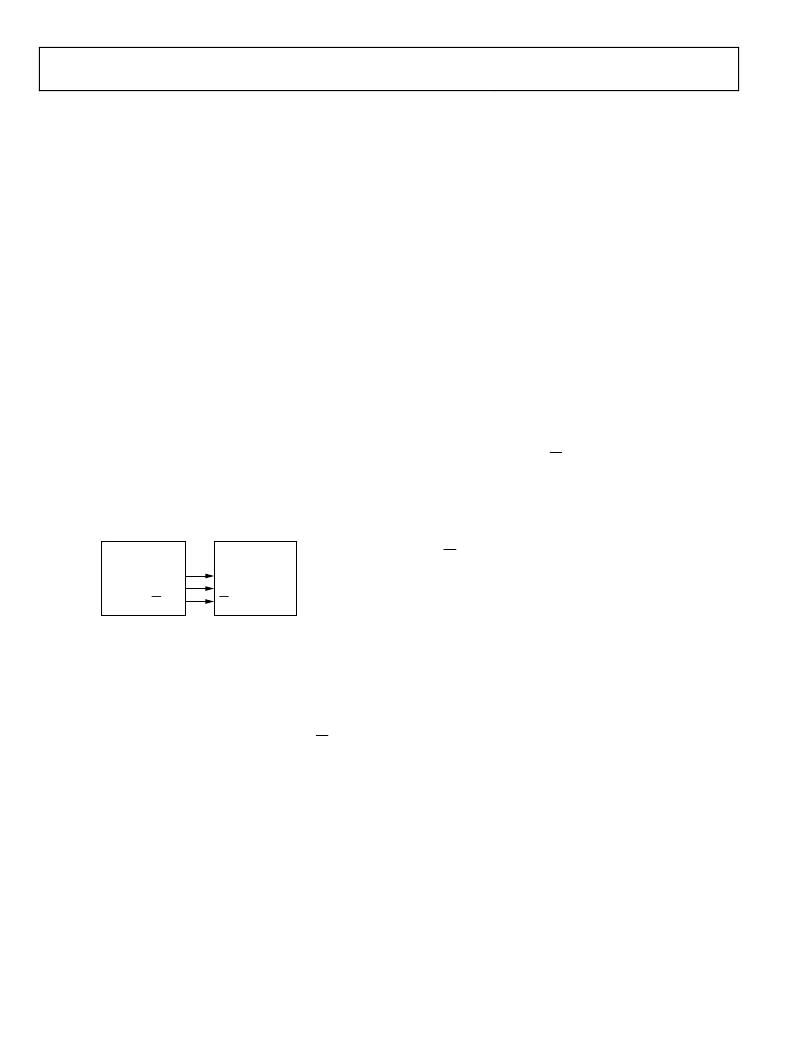
�ADE7816�
�MISO/HSD�
�HSCLK�
�SS/HSA�
�SPI� DEVICE�
�MISO�
�SCK�
�SS�
�E�
�A� A�
�This� means� that� HSA� stays� low� when� no� communication� is� in�
�progress.� When� the� communication� starts,� HSA� goes� high� and�
�stays� high� until� the� communication� ends;� then� it� goes� back� to� low.�
�After� a� hardware� reset� or� power-up,� the� MISO/HSD� and� SS� /HSA�
�Figure� 43.� Connecting� the� ADE7816HSDCwithaSPI�
�The� HSDC� communication� is� managed� by� the� HSDC_CFG�
�register,� Address� 0xE706� (see� Table� 28).� It� is� recommended� that�
�the� HSDC_CFG� register� be� set� to� the� desired� value� before� enabling�
�the� port,� using� Bit� 6� (HSDCEN)� in� the� CONFIG� register.� In� this�
�way,� the� state� of� various� pins� belonging� to� the� HSDC� port� do� not�
�take� levels� that� are� inconsistent� with� the� desired� HSDC� behavior.�
�E�
�A� A�
�pins� are� set� high.�
�Bit� 0� (HCLK)� in� the� HSDC_CFG� register� determines� the� serial�
�clock� frequency� of� the� HSDC� communication.� When� HCLK� is� 0�
�(the� default� value),� the� clock� frequency� is� 8� MHz.� When� HCLK� is� 1,�
�the� clock� frequency� is� 4� MHz.� A� bit� of� data� is� transmitted� for� every�
�HSCLK� high-to-low� transition.� The� slave� device� that� receives� data�
�from� HSDC� samples� the� HSD� line� on� the� low-to-high� transition�
�of� HSCLK.�
�Bits[7:6]� of� the� HSDC_CFG� register� are� reserved.� Any� value�
�written� into� these� bits� has� no� consequence� on� HSDC� behavior.�
��HXFER[1:0]� =� 01,� and� HSAPOL� =� 0.� Note� that� the� HSDC�
�interface� sets� a� data� bit� on� the� HSD� line� every� HSCLK� high-�
�to-low� transition,� and� the� value� of� Bit� HSIZE� is� irrelevant.�
��HGAP� =� 1,� HXFER[1:0]� =� 01,� and� HSAPOL� =� 0.� Note� that� the�
�HSDC� interface� introduces� a� gap� of� seven� HSCLK� cycles� between�
�every� 32-bit� word.�
��HGAP� =� 1,� HXFER[1:0]� =� 01,� and� HSAPOL� =� 0.� Note� that� the�
�HSDC� interface� introduces� a� gap� of� seven� HSCLK� cycles� between�
�every� 8-bit� word.�
�See� Table� 28� for� the� HSDC_CFG� register� and� descriptions� for�
�the� HCLK,� HSIZE,� HGAP,� HXFER[1:0],� and� HSAPOL� bits.�
�Rev.� A� |� Page� 34� of� 48�
�发布紧急采购,3分钟左右您将得到回复。
相关PDF资料
EVAL-ADE7878EBZ
BOARD EVAL FOR ADE7878
EVAL-ADE7880EBZ
BOARD EVAL FOR ADE7880
EVAL-ADE7953EBZ
BOARD EVAL FOR ADE7953
EVAL-ADF4002EBZ1
BOARD EVAL FOR ADF4002
EVAL-ADG788EBZ
BOARD EVALUATION FOR ADG788
EVAL-ADM1021AEB
BOARD EVAL FOR ADM1021
EVAL-ADM1023EB
BOARD EVAL FOR ADM1023
EVAL-ADM1031EB
BOARD EVAL FOR ADM1031
相关代理商/技术参数
EVAL-ADE7854EBZ
制造商:Analog Devices 功能描述:EVALUATION BOARDS - Boxed Product (Development Kits)
EVAL-ADE7858EBZ
制造商:AD 制造商全称:Analog Devices 功能描述:Poly Phase Multifunction Energy Metering IC with per Phase Active and Reactive Powers
EVAL-ADE7878EBZ
功能描述:BOARD EVAL FOR ADE7878 RoHS:是 类别:编程器,开发系统 >> 评估演示板和套件 系列:- 标准包装:1 系列:PCI Express® (PCIe) 主要目的:接口,收发器,PCI Express 嵌入式:- 已用 IC / 零件:DS80PCI800 主要属性:- 次要属性:- 已供物品:板
EVAL-ADE7880EBZ
功能描述:BOARD EVAL FOR ADE7880 RoHS:是 类别:编程器,开发系统 >> 评估演示板和套件 系列:* 产品培训模块:Obsolescence Mitigation Program 标准包装:1 系列:- 主要目的:电源管理,电池充电器 嵌入式:否 已用 IC / 零件:MAX8903A 主要属性:1 芯锂离子电池 次要属性:状态 LED 已供物品:板
EVAL-ADE7880EBZ
制造商:Analog Devices 功能描述:ADE7880, ENERGY METER, 3 PH, SPI, I2C, E
EVAL-ADE7913EBZ
制造商:AD 制造商全称:Analog Devices 功能描述:3-Channel, Isolated, Sigma-Delta ADC with SPI
EVAL-ADE7953EBZ
功能描述:BOARD EVAL FOR ADE7953 RoHS:是 类别:编程器,开发系统 >> 评估演示板和套件 系列:- 标准包装:1 系列:PSoC® 主要目的:电源管理,热管理 嵌入式:- 已用 IC / 零件:- 主要属性:- 次要属性:- 已供物品:板,CD,电源
EVAL-ADF4001EBZ2
制造商:Analog Devices 功能描述:Evaluation Board For Pll Frequency Synthesizer 制造商:Analog Devices 功能描述:ADF4001 PLL SYNTHESIZER EVAL BOARD